- 您现在的位置:买卖IC网 > Sheet目录3891 > PIC18C801T-I/L (Microchip Technology)IC MCU ROMLESS A/D PWM 84PLCC
2001 Microchip Technology Inc.
Advance Information
DS39541A-page 115
PIC18C601/801
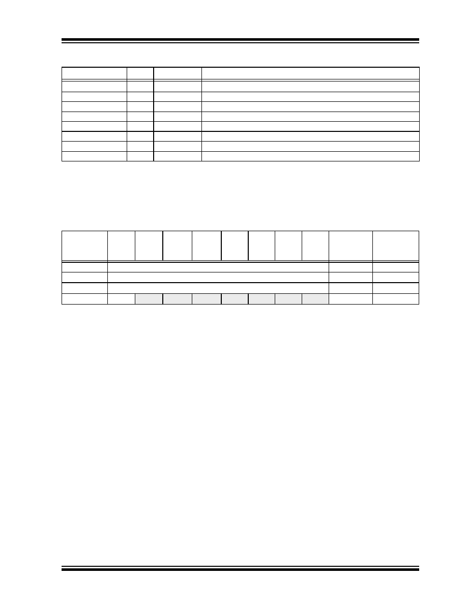
TABLE 9-9:
PORTE FUNCTIONS
TABLE 9-10:
SUMMARY OF REGISTERS ASSOCIATED WITH PORTE
Name
Bit#
Buffer Type
Function
RE0/AD8/A8(2)
bit0
ST/TTL(1)
Input/output port pin or Address/Data bit 8
RE1/AD9/A9(2)
bit1
ST/TTL(1)
Input/output port pin or Address/Data bit 9
RE2/AD10/A10(2)
bit2
ST/TTL(1)
Input/output port pin or Address/Data bit 10
RE3/AD11/A11(2)
bit3
ST/TTL(1)
Input/output port pin or Address/Data bit 11
RE4/AD12/A12(2)
bit4
ST/TTL(1)
Input/output port pin or Address/Data bit 12
RE5/AD13/A13(2)
bit5
ST/TTL(1)
Input/output port pin or Address/Data bit 13
RE6/AD14/A14(2)
bit6
ST/TTL(1)
Input/output port pin or Address/Data bit 14
RE7/AD15/A15(2)
bit7
ST/TTL(1)
Input/output port pin or Address/Data bit 15
Legend: ST = Schmitt Trigger input, TTL = TTL input
Note 1: Input buffers are Schmitt Triggers when in I/O mode and TTL buffers when in System Bus mode.
2: REx is used as a multiplexed address/data bus for PIC18C601 and PIC18C801 in 16-bit mode, and as an
address only for PIC18C801 in 8-bit mode.
Name
Bit 7
Bit 6
Bit 5
Bit 4
Bit 3
Bit 2
Bit 1
Bit 0
Value on:
POR,
BOR
Value on all
other
RESETS
TRISE
PORTE Data Direction Control Register
1111 1111
PORTE
Read PORTE pin/Write PORTE Data Latch
xxxx xxxx
uuuu uuuu
LATE
Read PORTE Data Latch/Write PORTE Data Latch
xxxx xxxx
uuuu uuuu
MEMCON
EBDIS
PGRM
WAIT1
WAIT0
—
WM1
WM0
0000 --00
Legend: x = unknown, u = unchanged. Shaded cells are not used by PORTE.
发布紧急采购,3分钟左右您将得到回复。
相关PDF资料
PIC18C658T-I/L
IC MCU OTP 16KX16 CAN 68PLCC
PIC18C658T-E/L
IC MCU OTP 16KX16 CAN 68PLCC
PIC16C925T-I/L
IC MCU OTP 4KX14 LCD DVR 68PLCC
PIC12F675-E/P
IC MCU CMOS 1K FLASH W/AD 8-DIP
PIC18C858T-E/L
IC MCU OTP 16KX16 CAN 84PLCC
PIC16F636-I/SL
IC PIC MCU FLASH 2KX14 14-SOIC
PIC18LC658T-I/L
IC MCU OTP 16KX16 CAN 68PLCC
PIC18LC801T-I/L
IC MCU ROMLESS A/D PWM 84PLCC
相关代理商/技术参数
PIC18C801T-I/PT
功能描述:8位微控制器 -MCU 2MB 1536 RAM 37I/O RoHS:否 制造商:Silicon Labs 核心:8051 处理器系列:C8051F39x 数据总线宽度:8 bit 最大时钟频率:50 MHz 程序存储器大小:16 KB 数据 RAM 大小:1 KB 片上 ADC:Yes 工作电源电压:1.8 V to 3.6 V 工作温度范围:- 40 C to + 105 C 封装 / 箱体:QFN-20 安装风格:SMD/SMT
PIC18C858-E/L
功能描述:8位微控制器 -MCU 32KB 1536 RAM 68I/O RoHS:否 制造商:Silicon Labs 核心:8051 处理器系列:C8051F39x 数据总线宽度:8 bit 最大时钟频率:50 MHz 程序存储器大小:16 KB 数据 RAM 大小:1 KB 片上 ADC:Yes 工作电源电压:1.8 V to 3.6 V 工作温度范围:- 40 C to + 105 C 封装 / 箱体:QFN-20 安装风格:SMD/SMT
PIC18C858-E/PT
功能描述:8位微控制器 -MCU 32KB 1536 RAM 68I/O RoHS:否 制造商:Silicon Labs 核心:8051 处理器系列:C8051F39x 数据总线宽度:8 bit 最大时钟频率:50 MHz 程序存储器大小:16 KB 数据 RAM 大小:1 KB 片上 ADC:Yes 工作电源电压:1.8 V to 3.6 V 工作温度范围:- 40 C to + 105 C 封装 / 箱体:QFN-20 安装风格:SMD/SMT
PIC18C858EPT
制造商:MICRO CHIP 功能描述:New
PIC18C858-I/L
功能描述:8位微控制器 -MCU 32KB 1536 RAM 68I/O RoHS:否 制造商:Silicon Labs 核心:8051 处理器系列:C8051F39x 数据总线宽度:8 bit 最大时钟频率:50 MHz 程序存储器大小:16 KB 数据 RAM 大小:1 KB 片上 ADC:Yes 工作电源电压:1.8 V to 3.6 V 工作温度范围:- 40 C to + 105 C 封装 / 箱体:QFN-20 安装风格:SMD/SMT
PIC18C858-I/PT
功能描述:8位微控制器 -MCU 32KB 1536 RAM 68I/O RoHS:否 制造商:Silicon Labs 核心:8051 处理器系列:C8051F39x 数据总线宽度:8 bit 最大时钟频率:50 MHz 程序存储器大小:16 KB 数据 RAM 大小:1 KB 片上 ADC:Yes 工作电源电压:1.8 V to 3.6 V 工作温度范围:- 40 C to + 105 C 封装 / 箱体:QFN-20 安装风格:SMD/SMT
PIC18C858T-E/L
功能描述:8位微控制器 -MCU 40MHz 16K OTP RoHS:否 制造商:Silicon Labs 核心:8051 处理器系列:C8051F39x 数据总线宽度:8 bit 最大时钟频率:50 MHz 程序存储器大小:16 KB 数据 RAM 大小:1 KB 片上 ADC:Yes 工作电源电压:1.8 V to 3.6 V 工作温度范围:- 40 C to + 105 C 封装 / 箱体:QFN-20 安装风格:SMD/SMT
PIC18C858T-E/PT
功能描述:8位微控制器 -MCU 32KB 1536 RAM 68I/O RoHS:否 制造商:Silicon Labs 核心:8051 处理器系列:C8051F39x 数据总线宽度:8 bit 最大时钟频率:50 MHz 程序存储器大小:16 KB 数据 RAM 大小:1 KB 片上 ADC:Yes 工作电源电压:1.8 V to 3.6 V 工作温度范围:- 40 C to + 105 C 封装 / 箱体:QFN-20 安装风格:SMD/SMT